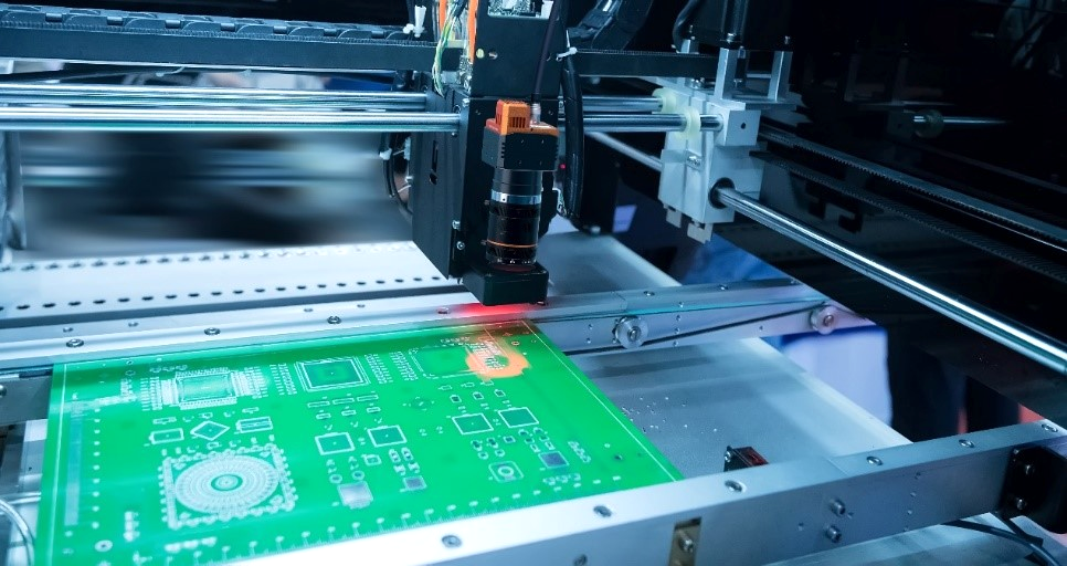
About hundreds of inspection points on the PCB board are coated with solder paste, in order to ensure product quality, it is necessary to detect the defects of solder paste on the PCB board, that is, to detect the covered area of solder paste.
Share
1). Project background:
Requirement description:
1. Originally, the method of surface array camera + two-dimensional moving robot arm was used for shooting, and the copper plate was stationary while the camera was moving; Visual inspection, can not save the picture, this scheme needs to add automatic recognition, data statistics and storage picture functions;
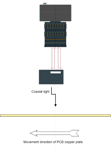
2. the copper plate has a mechanical structure to drive intermittent horizontal movement along the length direction; After the face array camera is completed, the copper plate is transported to the next station, so the line array camera can be set up between the two stations to shoot, and the copper plate passes at a uniform speed below;
3. the picture needs to be stored for two years, and it needs a large space hard disk to store it without compression; Therefore, it is necessary to increase the image compression function, output JPG format pictures, and establish indexes according to the production batch number to facilitate search.
Technical requirements:
1. the size of the copper plate is about 260*80mm, about 400 detection points above, are coated with solder paste;
2. The solder paste size is about 1mm*1mm.
2). Solution architecture:
The PCB defective product detection system uses linear array camera, FA industrial lens and coaxial light source to build a vision system, which is installed on the production line. The PCB board passes the image acquisition at a constant speed below. After the acquired image is sent to the vision processor, the algorithm tool of the vision system platform can detect whether each solder paste point has defects and the number of defects in all solder paste points.

3).Program advantages:
1. The scheme algorithm takes about 200ms, and can adapt to complex situations such as code deformation, imaging ambiguity, code hole imaging adhesion, and different code hole sizes.
2. each machine can recognize about 1000 boards per day, and the recognition rate of 8421 codes reaches 100% after debugging.
3. No deep learning modules are used to reduce costs.
4. can be reused for more PCB industry 8421 code identification needs.
