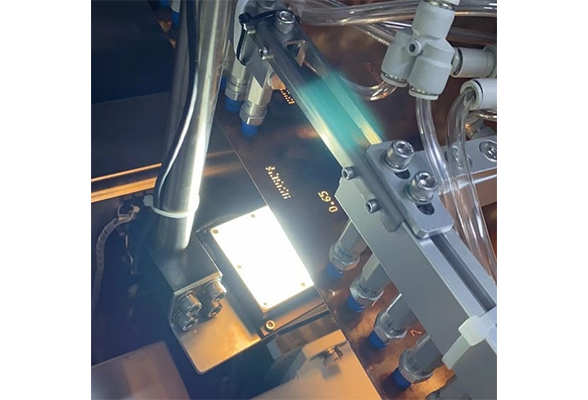
In the quality inspection part of this project, the voltage is measured by using two probes to poke both ends of the solder joints respectively, so as to judge whether the solder joints on the PCB board are in good contact and eliminate the problematic products.
Share
1). Project background:
Requirement description:
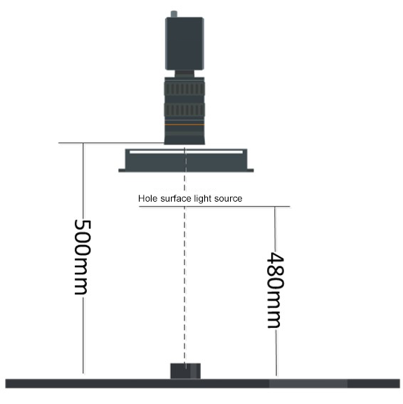
First, the PCB board is photographed by the upper camera, and the coordinates of the solder joints that need to be measured are given for rough positioning. Then the two manipulators respectively carry a probe to the corresponding coordinates to photograph the solder joint, perform precise positioning, and then poke the solder joint together to measure the voltage and determine whether the solder joint is good.
Pain points and problems:
1.Using the traditional scheme, the whole set of camera, lens, light source, light source controller and other costs are higher.
2.The traditional scheme has complicated process, high requirements for on-site debugging personnel, and high labor cost.
3.The traditional solution has a long debugging period and cannot be quickly launched.
2). Solution architecture:
Erection diagram:

Debugging process:
1. The manipulator carries the calibration sheet and maintains the same height with the PCB board. Take pictures on the camera, build the process with VM, receive the physical coordinates of the manipulator through TCP communication protocol, and carry out nine-point automatic calibration
2. The robot arm carries an intelligent camera to shoot the calibration board, carry out point-stamping, and generate calibration files through the images and physical coordinates of nine points
3. The PCB board position is sent to the robot arm, and the robot arm carries the smart camera to the corresponding position to photograph the solder joint
4. The smart camera uses spot search to frame each solder joint position in order, calibrate the coordinates and convert them to achieve sorting
5.After making the difference between the smart camera's calibration photo position and the production photo position, add the solder joint calibration conversion value to get the actual position of each solder joint
3). Program advantages:
1. Use an upper camera to take pictures of the coordinates of the manipulators on both sides directly, and the two manipulators reach the target point directly after taking pictures through calibration and transformation, and there is no need to go to it in turn, which greatly saves the time of manipulator movement. The whole process has been reduced from 15 seconds to about 5 seconds.
2. By reducing the rectangular box of the search solder joint and positioning each solder joint individually, it can be well positioned to the location of the solder joint. Customers require an accuracy of 0.1mm, and the current accuracy reaches 0.05mm to meet customer needs.
3. this project is a classic smart camera and industrial camera together to use the project, the actual project can be selected according to the actual needs of the appropriate type of camera, and even the two together to adapt to the customer environment, to achieve the corresponding effect.
4. The customer's original plan was to send coordinates to the corresponding position of the upper camera after taking the first picture, and send coordinates to the second picture after taking the second picture. The current plan only needs to take a picture once and call different calibration files to control the robot arm 1 and 2 at the same time, and the overall efficiency has been increased by 20%.