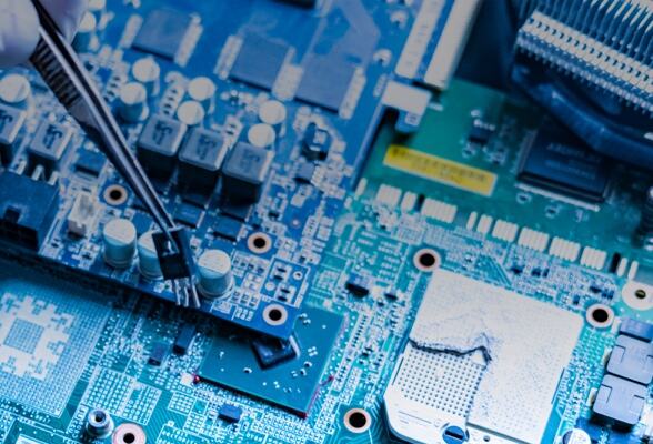
In the pre-middle process of semiconductor manufacturing, machine vision is mainly used in precision positioning and detection, and the post-process mainly involves the electrical detection, cutting, packaging, and detection of wafers. Machine vision helps the semiconductor industry to upgrade equipment, improve the process level of the production line, and improve the quality and yield of products, which is one of the core technologies of modern industry.
Share
Industry overview
1. Appearance inspection of electronic components
Detect the appearance of small electronic components, such as SMD products, silicon wafers
After high-speed and automatic photos are taken of the surface of the measured object, the data is transmitted to the computer for processing to find out the defective products, the types of defects include printing errors, content errors, image errors, direction errors, missed printing, surface defects, etc.

2. Check the chip appearance
Test IC chip size, appearance, flatness, etc
Check the number of pins and the geometric dimensions of multiple positions of pins, including pitch spacing, width, height, curvature, etc. To achieve continuous, efficient and rapid appearance detection of the chip, improve the detection efficiency, save labor costs and reduce the labor intensity of workers, and more importantly, ensure the accuracy of the detection.

3. PCB printed circuit detection
Detect PCB printed circuit board appearance size, position, defects, etc
Test PCB printed circuit board component position, solder joint, line, hole size, Angle measurement; Computer micro communication interface, SIM card slot; SMT component placement, surface mounting, surface detection; SPI solder paste inspection, reflow soldering and wave soldering; Check and measure the number of cable connectors and so on.
